~ Abdelrahman H. Ahmed. 9/2015 ~
SoC Encounter is an automatic place and route software from Cadence.
1 Environment Setup and starting Cadence SoC Encounter
The objective of this section is to learn how to get the environment ready for the tool, take care of the licensing issues, and start the tool.
1.1 SoC Encounter working Directory
In your Cadence tools directory, created in “RTL Compiler tutorial” section 1, descend into a folder called “PnR”. This folder will be the working directory for the Cadence SoC Encounter.
1.2 Get the needed files ready
To start the place and route (PnR) process you will need to provide the following files:
- The mapped Verilog file (Output from RTL Compiler).
Copy it to /PnR/in - The Output ‘SDC’ file from RTL Compiler
Copy it to /PnR/in - Locate the ‘.lib’ timing files.
The .lib files include the needed information about the standard cells.The path: /CMC/kits/AMSKIT616_GPDK/tech/gsclib045_all_v4.4/gsclib045/timing Needed files: “fast_vdd1v0_basicCells.lib” and “slow_vdd1v0_basicCells.lib”
- Locate the ‘.lef’ files.
The .lef files include the needed layout information about the standard cells.The path: /CMC/kits/AMSKIT616_GPDK/tech/gsclib045_all_v4.4/gsclib045/lef Needed files: “gsclib045_tech.lef”, “gsclib045_multibitsDFF.lef” and “gsclib045_macro.lef”
- Download “MMMC.tcl” [Piazza]
Contains the timing configurations. Make sure to edit it to point to your SDC file.
Copy it to /PnR/in - Download .map and .layermap files [Piazza]
Map the layers when importing the design from SoC encounter to Virtuoso.
Copy it to /PnR/in
1.3 Source the setup file and run SoC Encounter
In the working directory source the provided Setup file. Sourcing this file will take care of all the needed environment variables, and all the licensing as well. After sourcing the setup file, launch the tool.
| >> source ../setup_local.csh >>encounter -64 -log Mylog |
After running the previous lines Encounter should open its main window as in Figure 1. Read the log in the terminal to make sure that everything went well with no error.

Figure 1 Encounter’s main window
2 Place and Route the design
In this section follow the steps to convert your synthesized Verilog file into a layout.
2.1 Design import
In this step you will be configuring the tool and loading your design. Go to <File -> Import design>. The Design import screen shown in Figure 2 will open. Fill in the fields as follows:
Netlist: Select Verilog and browse to your mapped .v file, and Set the name of your Top cell.
Technology/Physical Libraries: Select LEF Files and browse to “add” the .lef files mentioned previously. Make sure to add them in order one by one as shown in Figure 3.
Power: Set the power and ground nets to VDD and VSS, respectively.
Analysis Configuration: Add your modified “MMMC.tcl”.
Finally save this configuration, and press OK. Note the change in Encounter’s main window.
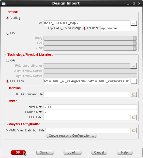
Figure 2 Design Import window

Figure 3 Add .lef files
2.2 Floorplan
In this step you will select the dimensions of your Layout, the utilization, and the IO ring space. Go to <Floorplan -> Specify Floorplan>. The Specify floorplan window shown in Figure 4 will open. Specify your desired parameters. Note that as you increase the Core utilization your design will have smaller area but this will make it more difficult for the routing tool to accomplish a clean routing with no LVS errors. Press Ok and notice the change in Encounter’s main window.
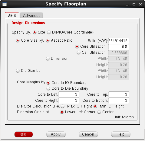
Figure 4 Specify Floorplan window
2.3 Save design
It is beneficial to save your design after each step, in case you want to start again from a specific point instead of repeating the whole process from the beginning. To do so, go to <File -> Save Deign…> and select the data type to be Encounter.
2.4 Power Planning
In this step you will be designing the power distribution network (PDN) for your design. The PDN should be designed in a way that provides power connection to each cell with minimum IR drop.
2.4.1 Power Rings
In this step you will create VDD and VSS ring that will surround your deign. Go to <Power->Power Planning -> Add Ring…>. This will open the Add Rings window shown in Figure 5. In the Net(s) field add VDD and VSS and pick your desired ring configuration settings. Press Ok.
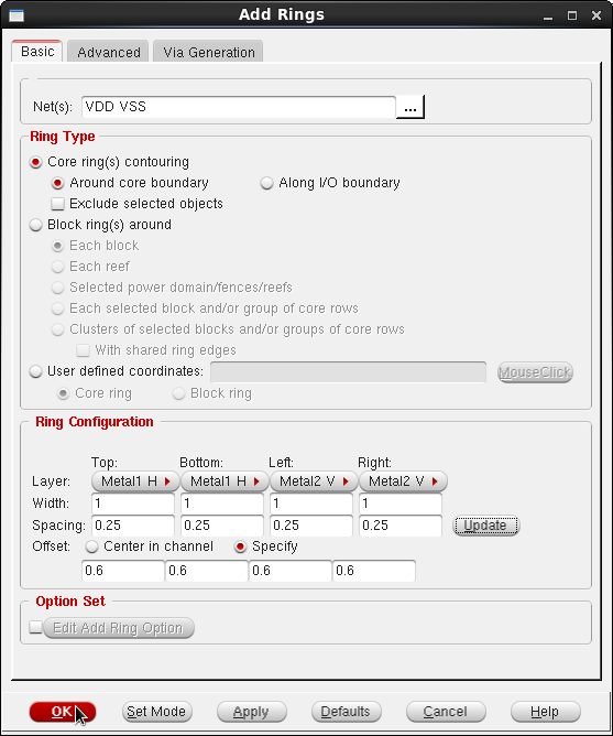
Figure 5 Add Power Rings
2.4.2 Power Stripes
In this step you will complete the PDN by adding VDD and VSS stipes that will cover the whole PnR area. First go to <Route-> Special Route> in the SRoute window shown in Figure 6 add VDD and VSS to the Net(s) field and press ok. Then, if needed, you can add more vertical connections to your PDN. Go to <Power->Power Planning-> Add Stripe…>. This will open the Add Stripes window shown in Figure 7. Add the VDD and VSS nets, select your desired settings, and press OK.
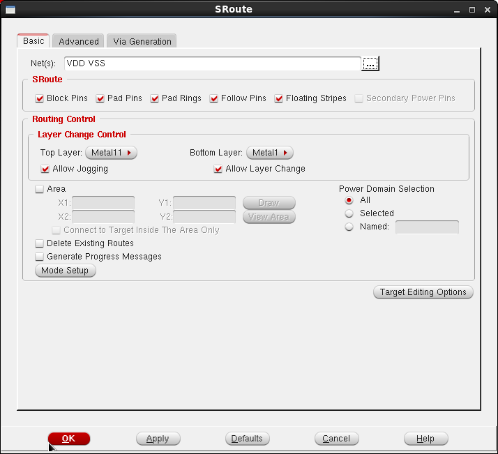
Figure 6 Special route for power and ground
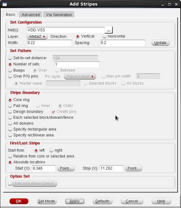
Figure 7 Add vertical power and ground stripes
2.5 Pin Placement
In this step you will specify the locations for the pins used in the design. Go to <Edit -> Pin Editor>. This will open the Pin Editor window shown in Figure 8. From the Pin Group list select each pin and specify its location and the metal layer assigned to it. Press ‘Apply’ after editing each pin. After this step your design should look similar to the one shown in Figure 9.
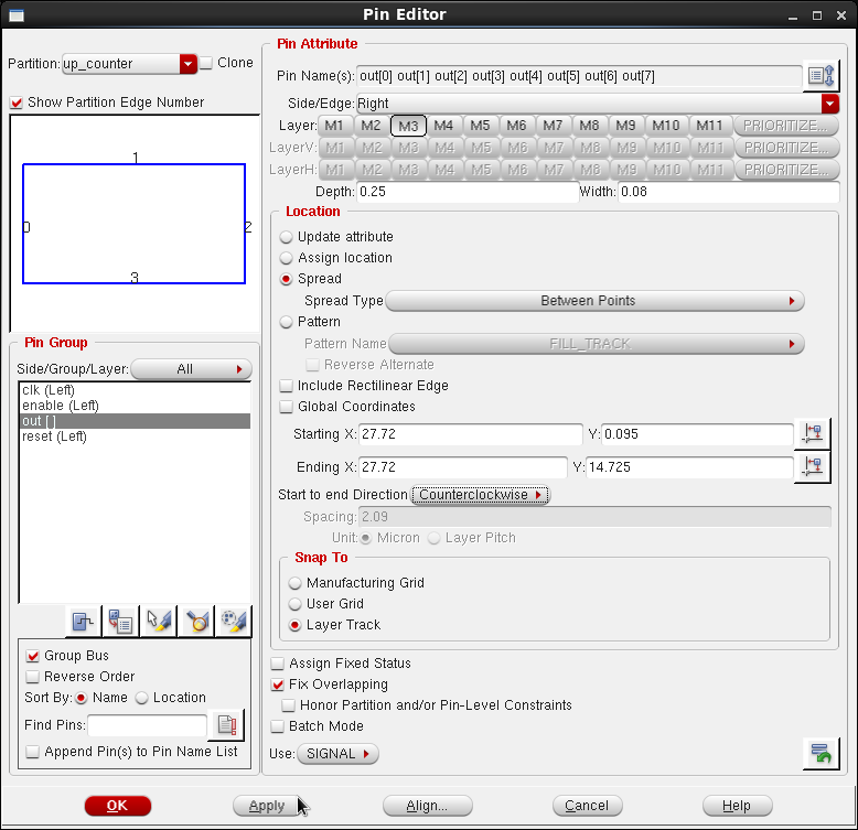
Figure 8 Pin Editor
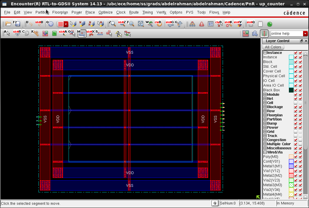
Figure 9 Layout after PDN and Pin planning
2.6 Standard Cells placement
To place the standard cells used on your design go to <Place -> Place Standard Cells>. The Place window shown in Figure 10 will open. Select “Include In-Place Optimization” then in the Mode Setup window shown in Figure 11 uncheck “Place IO Pins”. To see the effect after the placement step toggle between the different views using ![]() that can be found in the top left corner. When you go back to the Physical view your design should look similar to Figure 12. Note that the tool has created an initial routing between the cells.
that can be found in the top left corner. When you go back to the Physical view your design should look similar to Figure 12. Note that the tool has created an initial routing between the cells.
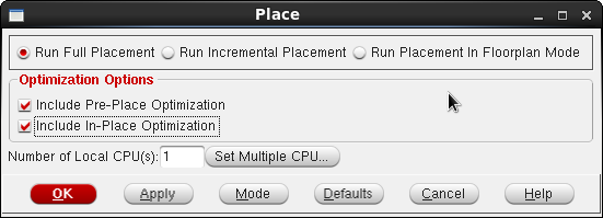
Figure 10 Standard cells placement
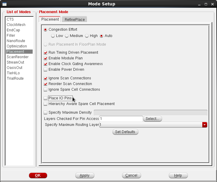
Figure 11 Placement Mode setup
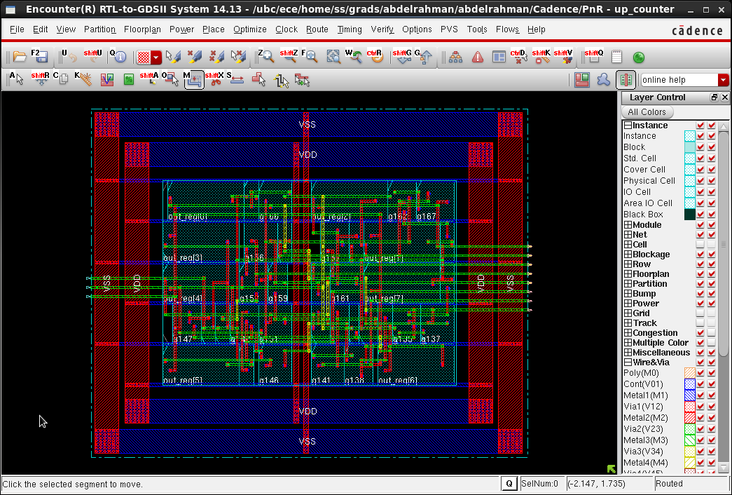
Figure 12 Layout after placement
After placing the standard cells there could be some gaps between them which might cause DRC errors. Filler cells could be added to solve this problem. Go to <Place -> Physical Cell -> Add Fillers…>. In the Cell Name(s) field go to select and add some of the available filler cells and the Dcaps. Press OK, and make sure that your design does not have any gaps. Note that the numbers in the filler cells name are indication to their sizes, so make sure that your selection includes both big and small filler cells.
2.7 Route
Go to <Route -> NanoRoute-> Route…>. In the NanoRoute window select “Timing Driven” and press Ok. In the terminal make sure that the routing was done successfully with no fails of errors.
2.8 Verification
The final step is to verify that your design passes the Geometry and Connectivity check, which are equivalent to DRC and LVS checks. Go to <Verify -> Verify Geometry…>, and press OK in the Verify Geometry window. Check the terminal to make sure that your design has zero violations as shown in Figure 13. Similarly, verify the connectivity and make sure that the design has zero connectivity violations as shown in Figure 14.

Figure 13 Verify Geometry results

Figure 14 Verify Connectivity results
3 After the PnR
After finishing the PnR process it is desirable to do post PnR simulation which requires the generation of timing file (.sdf) that could be used in ModelSim. Furthermore, it is desirable to import the layout to Cadence Virtuoso for the top-level use.
3.1 Generate .sdf file
Go to <Timing -> Extract RC>, select all the items, and press OK. In the terminal type [write_sdf Up_counter.sdf] to generate the SDF file. This file can be used in ModelSim as explained in RTL Compiler tutorial.
3.2 Import the design to Virtuoso
Go to <File-> Save-> GDS/OASIS>. In the Output File name use [./out/up_counter.gds], and for the Map File use[/in/gds2.map]. Keep the rest as default and press OK.
Open Virtuoso, and create a new library as described in the Cadence Virtuoso tutorial. In the CIW go to <file -> import -> Stream…>, and fill in the fields in the stream in window as follows:
*Stream file: Browse to your .gds file.
*Library: Select the library you just created.
*Top Level Cell: Add the name of your top module.
*Press show options.
**In the layers tab load [gsclib045_tech.layermap].
**In the libraries tab add the “gsclib045” to the reference libraries using the GUI arrows.
Finally, press translate. In the library you will be able to find the imported layout of your design.