~ Spoorthi Nayak and Abdelrahman H. Ahmed. 9/2015 ~
Virtuoso is a schematic and layout editor software from Cadence.
1 Environment Setup and starting Cadence Virtuoso
The objective of this section is to learn how to get the environment ready for the tool, take care of the licensing issues, and start the tool.
1.1 Virtuoso working Directory
Open the terminal to create and source the Setup file.
>> mkdir HighSpeedIO — Creating the Working Directory
>> cd HighSpeedIO — Desending into the Working Directory
1.2 Source the setup file and run Cadence
In the working directory source the provided Setup file. Sourcing this file will take care of all the needed environment variables, and all the licensing as well. After sourcing the setup file, launch the tool.
>> source /CMC/scripts/kit.tsmc65nm_gp_OA.2.1.csh
>> virtuoso –log Mylog&
After running the previous lines Cadence should open its main window as in Figure 1, also known as Command Interpreter Window (CIW). Read the log in that window to make sure that everything went well with no errors or warnings.
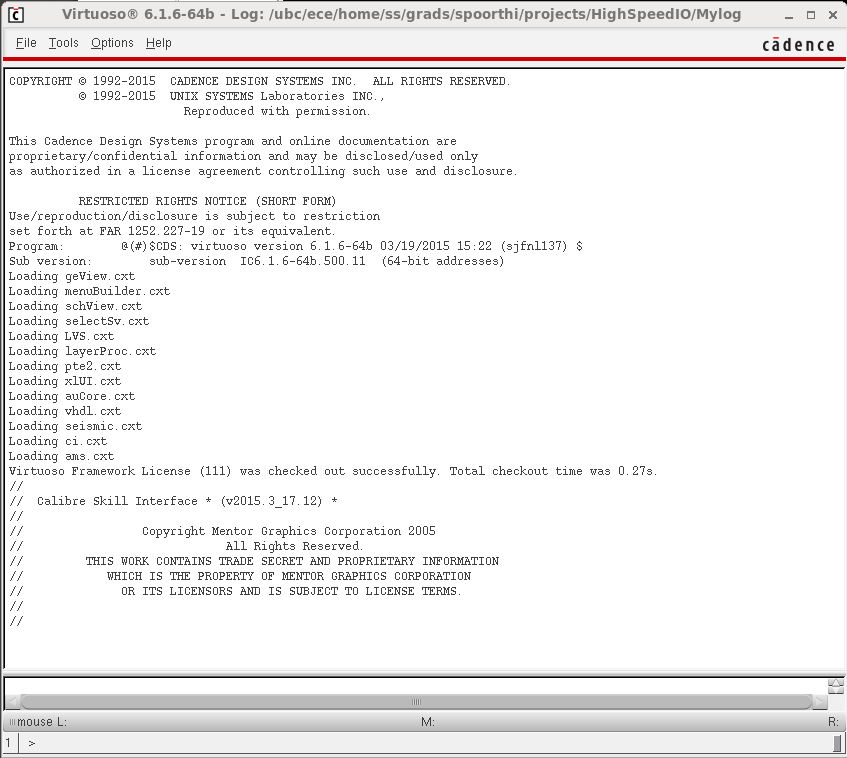
Figure 1 Cadence Virtuoso’s CIW.
2 Cadence Virtuoso Schematic and Symbol Editors
The objective of this section is to know how to create a new project, create a new schematic, and simulate it.
2.1 Create a new library
In cadence virtuoso the “library” is your project directory. The “library” can have multiple sub-projects each is called a “cell”. The “cell” can have multiple views like (Schematic, layout … etc.). Each project will be created using a certain Process Design Kit, also known as PDK, so the “library” should be linked to the used PDK.
To create a new library, first go to <Tools –> Library Manager…> to open the “Library Manager” window. In the “Library Manager” go to <File –> New –> Library…>, this will open a new window asking for your new library’s name. Select a name for your library, which was named HighSpeedIO in this tutorial, and select “Attach to an existing technology library” under Technology File, then press Ok. A new window asking for the technology Library for your new library will show up. Select “tsmcN65” and press OK.
2.2 Create a new schematic
Now inside your project library create a new schematic for a sub-cell. Select your project library, and go to <File –> New –> Cell View…>. A new window asking for details about your new cell view will open. Make sure to pick a name for your cell that describes its functionality and highlights any other important details about that cell. Also, make sure that the ‘View’ and ‘Type’ fields are set to schematic and then press OK. Now the Schematic Editor window will open as in Figure 2, and the Library Manager window will indicate the changes you just made as in Figure 3.
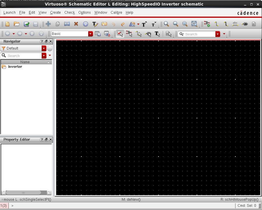
Figure 2 Virtuoso Schematic Editor.
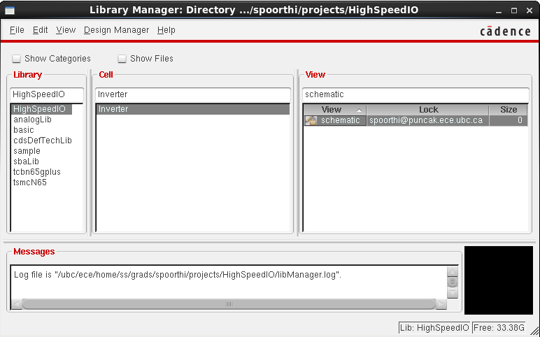
Figure 3 Library Manager window after creating a new schematic.
Start exploring the Schematic Editor window, and note that to create a new schematic most of the needed options can be found in “Create” drop-down menu. Note that every action can be either done through the Create menu, the GUI buttons in the tool bar, or using hot keys. For example, to add a new instance go to <Create –> Instance…>, use![]() icon from the tool bar, or just hit “I”. You can learn about the actions and their corresponding icons and hot keys from the Create menu. To change the parameters of any device, select the device and press “Q”.
icon from the tool bar, or just hit “I”. You can learn about the actions and their corresponding icons and hot keys from the Create menu. To change the parameters of any device, select the device and press “Q”.
After creating the schematic go to <File –> Check and Save> or use its equivalent short cuts. Make sure that your schematic has no errors or warnings, and then proceed.
To prepare the schematic to be used to create a symbol for your cell, make sure to use Pins for your inputs, outputs, and supply and ground. Figure 4 shows the schematic of an inverter, which is ready to be used in symbol creation. Note that inputOutput pin type was used for the supply and the ground.
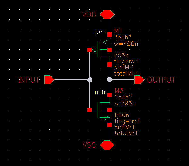
Figure 4 A schematic of a CMOS inverter.
2.3 Create a symbol
Having a symbol for each cell in a project is a very powerful tool that makes test benches and larger systems creation an easy task.
For an errors and warnings-free schematic with all ports assigned to pins go to <Create –> Cellview –> From Cellview> in the Schematic Editor. The “Cellview from Cellview” window will open. Make sure that the ‘To View Name’ field is set to symbol and press OK. This will open the “Symbol Generation Options” window in which you can select the desired Pin specification as shown in Figure 5. Make the desired changes and press OK. The Symbol Editor window shown in Figure 6 will open.
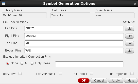
Figure 5 Symbol Generation Options window.
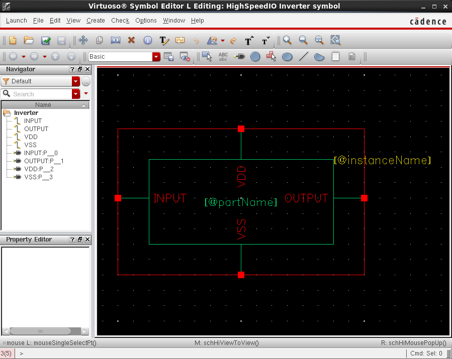
Figure 6 Virtuoso Symbol Editor.
Start exploring the Symbol Editor window, and note the similarities between it and the Schematic Editor window. Use the shapes creation tools that can be found in “Create” drop-down menu, to create a symbol for your cell. Note that the symbol should reflect the functionality of the cell and highlight its main features. Figure 7 shows a symbol of a CMOS inverter.

Figure 7 A symbol for a CMOS inverter.
Note: Sometimes it could be helpful to change the snap spacing. To change it press “O” to open the “Display Options” window.
After creating the symbol go to <File –> Check and Save> or use its equivalent short cuts. Make sure that your symbol has no errors or warnings, and then proceed.
3 Simulation using Analog Design Environment
The objective of this section is to learn how to create test benches for some of the basic simulations need to characterize digital standard cells using Cadence Virtuoso Schematic Editor and Analog Design Environment, known as ADE, simulation tool.
3.1 Create a test bench
A test bench is simply a schematic that includes the cell under test and some assisting instances, like voltage sources and current sources. Most of the needed instances to create a test bench can be found in analogLib library.
To create a test bench schematic follow the same steps as in section 2.2 and name it <cell_TB>. Add the assisting instances depending on the test type as discussed in the following sections.
3.2 Basic simulations for a CMOS inverter
In this section, some of the basic simulations and test benches for a CMOS inverter will be discussed. These simulations could be helpful with other digital cells as well, and will help you in creating a database of information about your digital cells.
3.2.1 Transient simulation
In this section you will be simulating the inverter to check its functionality, visualize the input and output waveforms, and to calculate its delay, rise, and fall times.
First, create a Test Bench schematic for the inverter’s transient simulation as shown in Figure 8. The used instances in this TB are (INVERTER from ELEC402 library) and (cap, vdc, gnd, and vpulse from analogLib library).
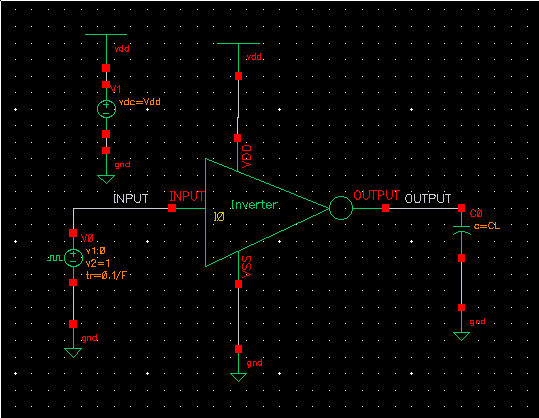
Figure 8 Transient simulation test bench for a CMOS inverter.
Note: Giving the assisting instances’ parameters “variable names” can be helpful when using ADE to simulate the TB. Doing that will make it easy to control all the TB parameters from only one place.
Fill in the parameters of the ‘vpulse’ and ‘vdc’ instances as shown in Figure 9. With the same method give ‘cap’ a variable value of CL in the capacitance field.
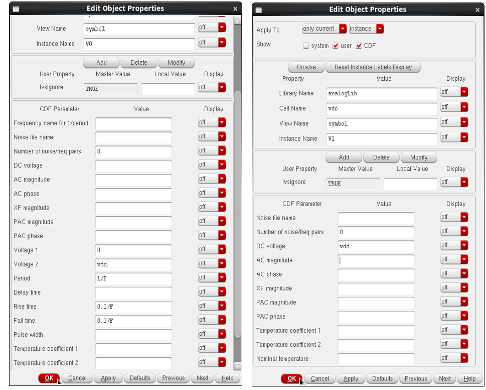
Figure 9 Left (vpulse properties). Right (vdc properties).
To start simulating the test bench go to <Launch –> ADE L> in the Schematic Editor window. This will open the ADE window shown in Figure 10. In the ADE window follow the following steps to prepare it for the simulation:
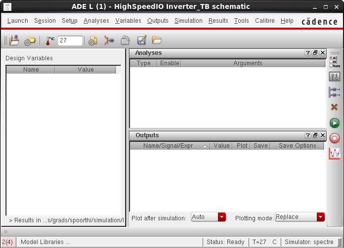
Figure 10 ADE window.
- Import the design variables and give them the desired values:
Go to <Variables –> Copy From Cellview>. Note that your design variables are added to the “Design Variables” section in the ADE window. Fill in the ‘Value’ fields with the desired numbers as shown in Figure 12. - Set the required Analyses:
Go to <Analyses –> Choose …>. In the new window select ‘tran’ analysis and set the analysis properties as shown in Figure 11. Note the change in the “Analyses” part in the ADE window as shown in Figure 12. - Select signals to be plotted:
Go to <Outputs –> To Be Plotted –> Select On Design>. In the schematic click on the ‘INPUT’ and ‘OUTPUT’ wires and then press ‘Esc’. Note that these signals were added to the “Outputs” part in the ADE window as shown in Figure 12.
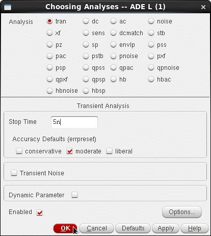
Figure 11 Transient analysis setup.
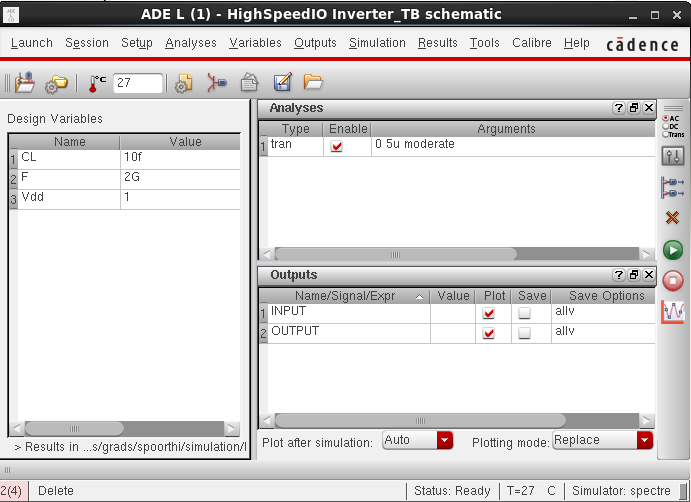
Figure 12 ADE window after transient analysis setup.
After doing the previous steps your TB is now ready. Go to <Simulation –> Netlist and Run>. Note that two windows will open, the simulation log and the waveform visualization window. Check the simulation log to make sure that everything went well with no errors.
Explore the visualization window, and specially the ‘View-Graph-Marker’ drop-down menus. Prepare the wave forms for measurement by:
- Go to <Graph à Split Current Strip>, to separate the graphs as shown in Figure 13.
- Press “X” and then with the right mouse button clicked drag a window that includes two cycles then release to zoom to that area.
- Start adding markers by pressing “M” while pointing with the cursor to the required point. To edit the marker values double click on it.
- To add differential marker between two points press “M” at the first point and then “D” at the second point.
Using the previous tips try to get the delay, rise, and fall times as shown in Figure 13.
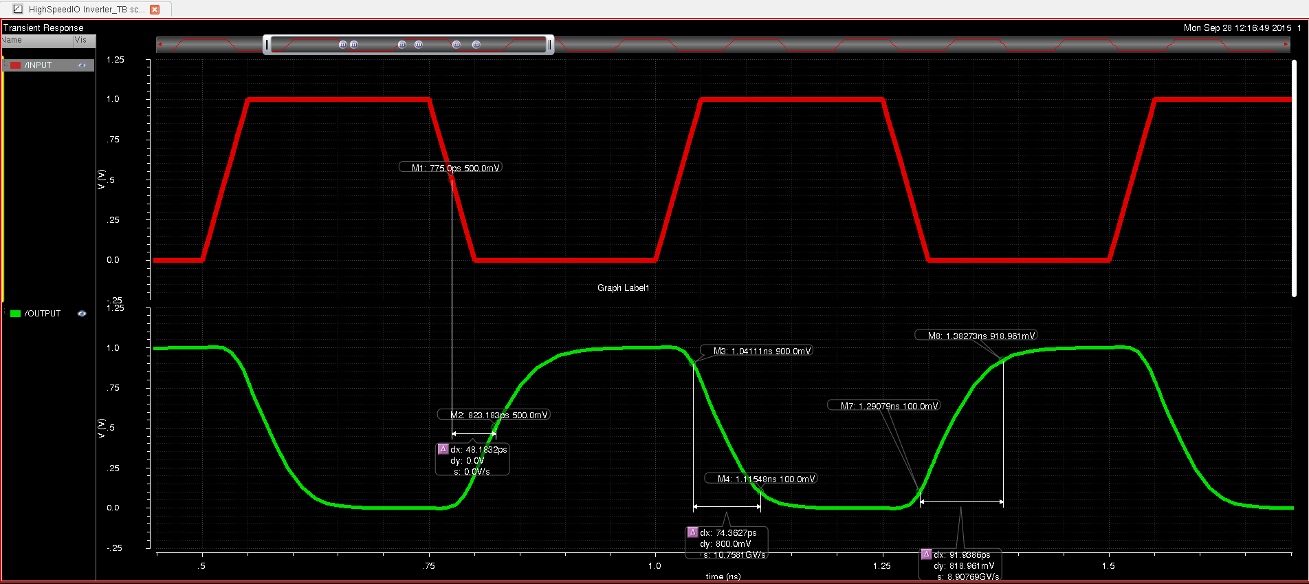
Figure 13 Waveforms of the inverter’s INPUT and OUPUT signals.
Note from Figure 13 that the delay, rise and fall times are 48.18ps, 91.93ps and 74.39ps, respectively. Which is not a good design, WHY?!!
Another alternative to using the markers in determining these values is to use the “Calculator” tool. To open the calculator go to <Tools –> Calculator>. Note all the functions that can be done using it in the “Function Panel” part.
As an example, the rise time of the output signal can be measured using the following steps:
- Select
 and then in the visualization window click on the output wave form.
Note that this line will be added to the Calculator window <clipX(v(“/OUTPUT” ?result “tran”) 449.0E-12 1.701E-9 ) >
- In the Function Panel look for “riseTime” and click it.
- Set the rise time function properties as shown in Figure 14 and press OK. The line will change to <riseTime(clipX(v(“/OUTPUT” ?result “tran”) 449.0E-12 1.701E-9 ) 0 nil 1 nil 10 90 nil “time” )>.
- Finally, press
 to evaluate the rise time value.
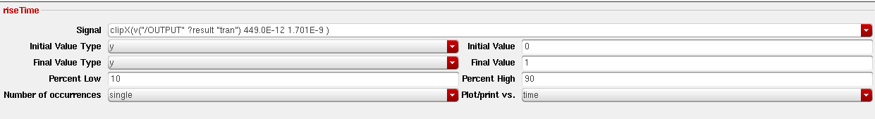
Figure 14 Rise Time function properties in the “Calculator”.
Note: one of the most effective uses of the “Calculator” in evaluating simulated signals comes when the design variables are being swept.
Finally, to save your simulation setup for latter use go to <Session –> Save State>. Fill in the required fields as shown in Figure 15 and press OK. To load your saved simulation setup go to <Session –> Load State>, then browse the desired state and press OK.
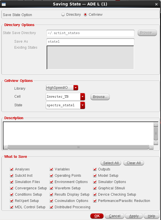
Figure 15 Save State window.
3.2.2 DC Simulation
This simulation is mainly used to check the DC-operating points of different devices in the design. Another very important use for it is while sweeping one of the variables in the system and monitoring the changes in one, or more, of the circuit parameters.
As an example in this tutorial DC simulation will be used to plot the inverter’s characteristic curve. The characteristic curve can be helpful in determining the inverter’s threshold voltage, noise margins, and its gain. First, change the TB created in 3.2.1 by placing a ‘vdc’ at the input of the inverter instead of the ‘vpulse’. In the new ‘vdc’ set the the ‘DC voltage’ field to vin.
Open a new ADE window and follow the following setup steps:
- Import the design variables and give them the desired values:
Go to <Variables –> Copy From Cellview>. Note that your design variables are added to the “Design Variables” section in the ADE window. Fill in the ‘Value’ fields with the desired numbers as shown in Figure 17. - Set the required Analyses:
Go to <Analyses –> Choose …>. In the new window select ‘dc’ analysis and set the analysis properties as shown in Figure 16. Note the change in the “Analyses” part in the ADE window as shown in Figure 17. - Select signals to be plotted:
Go to <Outputs –> To Be Plotted –> Select On Design>. In the schematic click on the ‘INPUT’ and ‘OUTPUT’ wires and then press ‘Esc’. Note that these signals were added to the “Outputs” part in the ADE window as shown in Figure 17. - Save the state
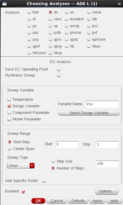
Figure 16 DC Analysis setup.
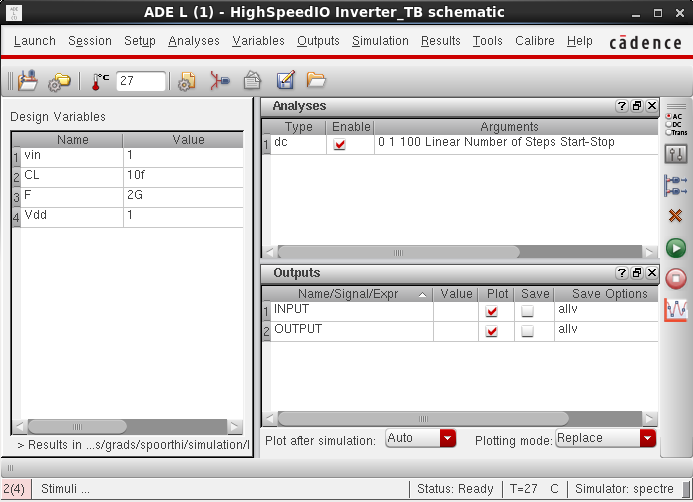
Figure 17 ADE window after DC analysis setup.
After doing the previous steps your TB is now ready. Go to <Simulation –> Netlist and Run>. Note that two windows will open, the simulation log and the waveform visualization window. Check the simulation log to make sure that everything went well with no errors.
Figure 18 shows the CMOS inverter’s characteristic curve. The derivative of the curve can be more informative. So using the “Calculator” tool plot the derivative using the following steps:
- Go to <Tools –> Calculator> to open the calculator.
- Select and then in the visualization window click on the output wave form.
Note: this line will be added to the Calculator window < v(“/OUTPUT” ?result “dc”) > - In the Function Panel look for “deriv” and click it.
- The line will change to < deriv(v(“/OUTPUT” ?result “dc”))>.
- Finally, press to plot the derivative as shown in Figure 19.
From Figure 19 many information about the design can be interpreted. What is the Value of the inverter’s threshold voltage, noise margins, and gain?
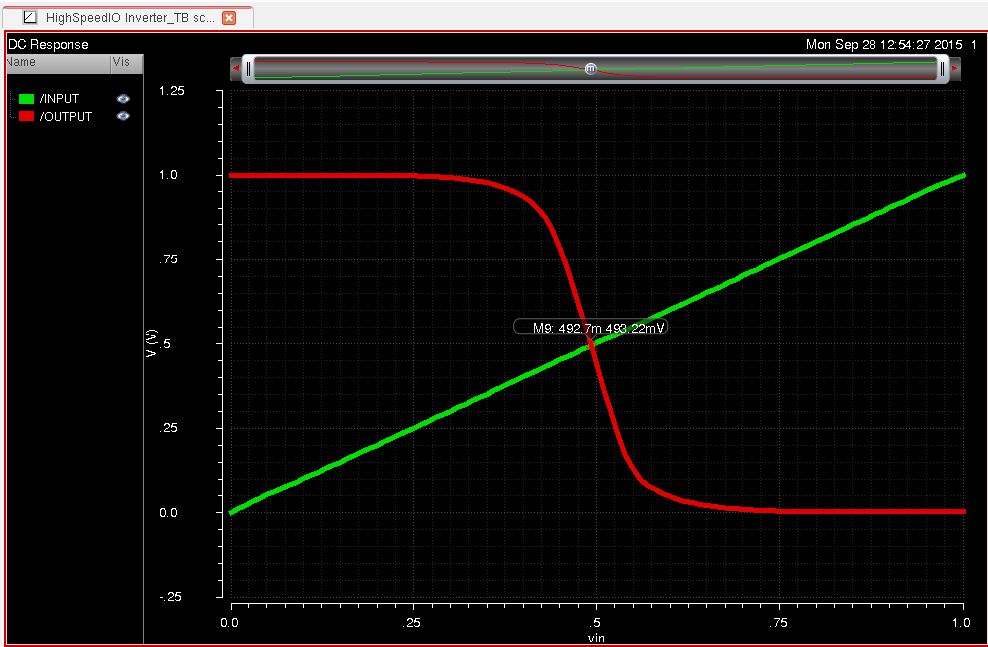
Figure 18 CMOS inverter’s characteristic curve.
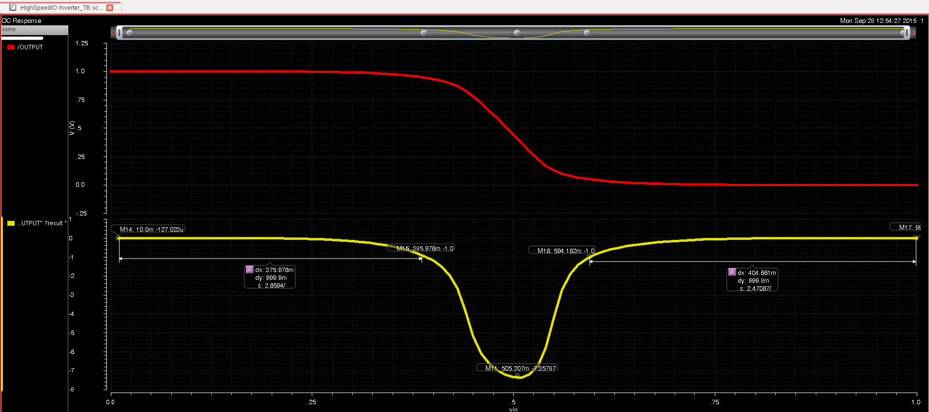
Figure 19 Derivative of the inverter’s characteristic curve.