Our research is focused on integrated systems and circuits, with applications in the area of optoelectronics, high-speed interconnects, wireless systems, and sensing. As such, we are often investigating challenges that fall at the intersection of circuits and communication systems, photonics, computer architecture, physics, quantum mechanics, signal processing, computing and machine learning.
Major Research Thrusts:
Narrow Linewidth Lasers and Isolator-Replacements
Silicon photonics on CMOS SOI has come a long way in the last 10 years. Two glaring omissions include: co-integrated laser (in foundries except Intel) and on-silicon isolators.
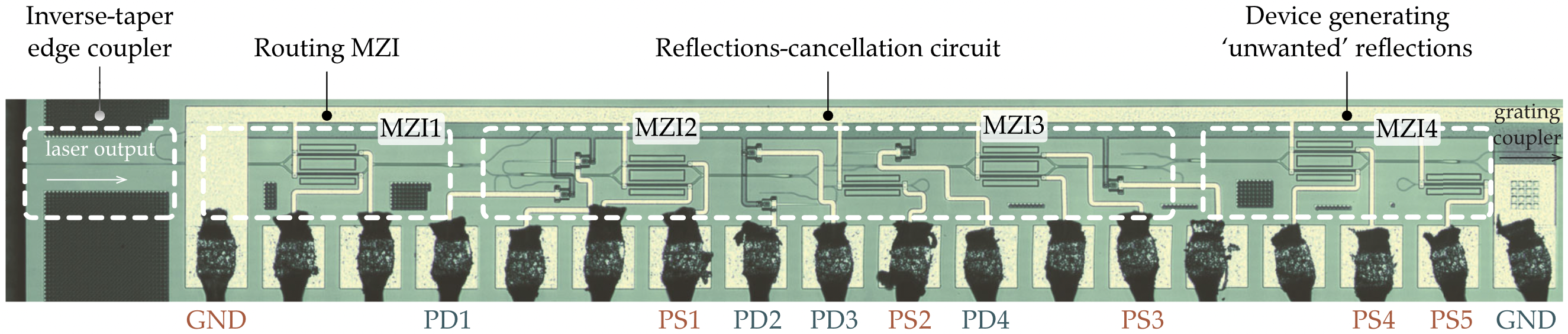
Isolators block unwanted back reflections and ensure the stable operation of the laser. For most optical systems employing a laser, magneto-optic isolators have been indispensable, but such isolators are incompatible with silicon. We are working on CMOS-controlled reflections-cancellation circuits as a way to reduce the reflections going back to the laser and keep the laser stable. Our recent work [ShomanJLT21] demonstrated a stable quantum well (QW) distributed feedback (DFB) laser against time-varying reflections using a reflections-cancellation circuit (RCC) on a zero-change, foundry-produced, silicon-photonic (SiP) chip. The optical spectrum and the relative intensity noise (RIN) of the laser when the RCC was running is comparable to when an isolator was used.
A low-cost, high-performance laser will pave the way towards the mass production of fully integrated, low-cost electronic-photonic silicon chips. Using self-injection locking, and by accurately locking the laser in a stable optical feedback regime, the performance of the laser can be significantly improved, and its linewidth and phase noise reduced by orders of magnitude. Our ongoing research is focussed on solving the laser and isolator challenges of silicon photonics using a combination of photonic, electronic and integration techniques.
Optoelectronics Transceivers:
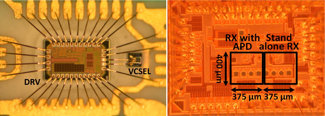 Majority of optoelectronics links in datacenters employ 850 nm wavelength VCSELs and photodetectors (PDs) for interconnects spanning a length of few meters up to 300 m [AhmedJSTQE16]. With newer standards focusing on higher data rates and advanced modulation schemes such as pulse amplitude modulation (PAM4), effects such as reliability, bondwires, linearity and crosstalk must be carefully addressed in the system design for an energy-efficient link design. We recently presented a differential push-pull voltage-mode VCSEL driver and demonstrated that it mitigates the challenges of high power consumption, sensitivity to packaging and incompatibility to advanced CMOS process scaling. Our prototype has achieved the highest ever-reported power conversion efficiency for VCSEL drivers when normalized to VCSEL slope efficiency [RamaniTCAS19]. At the receiver (RX) side, we have recently demonstrated a monolithically integrated Avalanche Photodetectors and transimpedance amplifier (TIA) in a standard 0.13um CMOS process. Fully monolithic integration relaxes many challenges associated with traditional APDs. The RX achieved a sensitivity of -18.8 dBm, the best-reported among 10 Gb/s linear CMOS TIAs operating at 850 nm [NayakTCAS19].
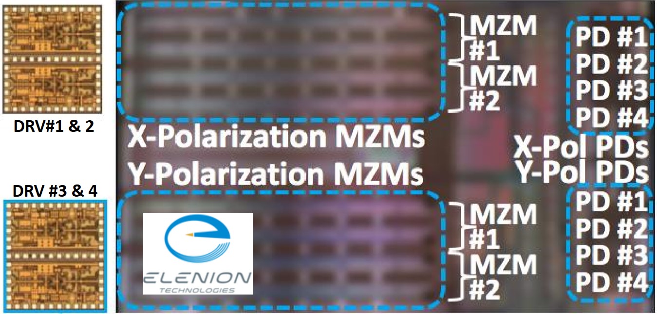 Silicon photonics has now emerged as a potential disruptive technology for meeting the bandwidth requirements of medium-to-long reach interconnects for datacenters. Derived from the mature CMOS fabrication technology, silicon photonics fabrication provides a platform where optical signals can be efficiently manipulated at large scales using inexpensive and densely integrated components on-chip. Our research efforts include design of high-speed drivers and transimpedance amplifiers for various modulation schemes such as NRZ/PAM4/QPSK/QAM. Our recent work on coherent silicon photonic links, in collaboration with Nokia-Elenion demonstrated a data rate of > 0.5 Tb/s/wavelength on a silicon platform [AhmedISSCC19, AhmedJSSC20, AhmedJSSC23].
Our ongoing research is focussed on silicon photonic transmitters: high-bandwidth transmitters, low-power coherent transmitters, and next-generation modulators.
Inexpensive, Quantitative and Multiplexed Biosensors:
Can we democratize and decentralize medicine using silicon electronic-photonic integrated circuits? While commercial-grade platforms today offer quantitative gold-standard tests for nucleic acid and protein biomarkers, they require centralized laboratory analysis, trained technicians, long time-to-result, and expensive equipment. On the other hand, current rapid, low-cost assays like lateral-flow strips (e.g., pregnancy tests) tend to be qualitative, low-sensitivity and multiplexed to two. Biomarker testing cannot be ubiquitous until it reliably gives accurate, rapid, and cost-effective diagnoses in a user-friendly format.
Microchips can be built in the billions and cost pennies at such volume. Photonic microchips are highly sensitive biosensors to detect biomarkers, and the technology has already been proven commercially. Although the chips cost very little, the standard commercial-grade measurement equipment costs tens of thousands of dollars due to the use of a tunable laser, sits on a lab bench, and discards most of the data due to its inherent architectural limitations. Can we shrink the equipment to a portable, disposable, inexpensive testing kit device? Our multidisciplinary team (Cheung, Chrostowski, Grist) have made early breakthroughs to realize such a vision, and we look forward to sharing more results on this soon. Some teasers are described in [ChrostowskiSPIE21, GristSPIE23].
Frequency Synthesis and Distribution:
A survey of CMOS phase locked loops (PLLs) over the last two decades show that the overall performance of PLL based frequency synthesizers are bounded by a tradeoff between noise, area and power consumption. Analog Type-II PLLs are very popular due to their low noise performance, but are area and power hungry. All-digital PLLs are compact and friendly to technology scaling, but limited in noise performance under a restrained power budget.
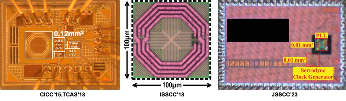
Our research is focused on using Type-I PLL to ease the tradeoffs, and achieve good noise performance in a compact footprint and low power budget. Overcoming the limitations of conventional Type-I topologies, our recent voltage-mode prototype demonstrated comparable performance to start-of-the-art architectures, but in an area of only 0.12 mm2 in 0.13-μm CMOS [SharkiaCICC15, SharkiaTCAS18]. This was followed by a sub-sampling Type-I architecture that achieved sub-200fs jitter in 1mW power in an area of 100µm x 100µm, thus proving for the first time that an LC PLL can beat the state-of-the-art power-performance benchmarks with an area of a ring-based PLL [SharkiaISSCC18, SharkiaJSSC18].
Our ongoing research is focussed on multi-phase clock generation and distribution, as well as new techniques for fractional frequency synthesis. We recently demonstrated a technique to improve the linearity of phase interpolators [MishraISSCC22, MishraJSSC23], useful for high-speed electrical receivers in advanced CMOS processes. We also went back to an old technique, Serrodyne Modulation, and demonstrated [SharkiaJSSC23] that it can be modified to realize a new energy-and-area efficient way to generate fractional frequency synthesis for different lanes of a wireline receiver.
CMOS Clocking for mm-wave Applications
The deployment of mm-wave portion of frequency spectrum (30 GHz to 300 GHz) for wireless applications is gaining tremendous popularity. The availability of wide bandwidth at the lower mm-wave bands (near 30 GHz, 60 GHz, etc.) makes these bands attractive for next generation mobile network. A key challenge in most CMOS communication systems operating at these bands is synthesis of on-chip LO frequency – with high spectral purity and large tuning range.
The upper mm-wave (200GHz and higher) and sub-THz bands are also attractive for applications such as medical imaging, non-invasive industrial testing and spectroscopy. Although CMOS promises a low-cost, portable platform for these applications, efficient power generation at these high frequencies faces daunting challenges on several fronts.
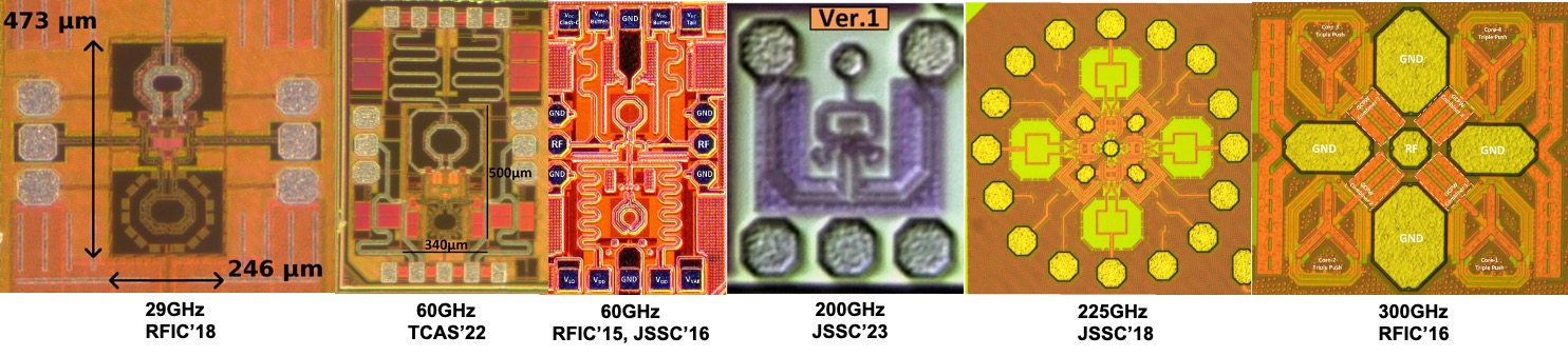
Our recent work has focused on using harmonics, mixing and multiplications for mm-wave clock generation in bulk CMOS processes. These include some of the most efficient and low-noise CMOS oscillators at ~30 GHz [LightbodyRFIC18, ShiraziCICC20, EsmaeeliTCAS22], 60 GHz [ShiraziJSSC16, EsmaeeliTCAS22], 200 GHz [Ghorbani-Nejad23], 225 GHz [NikpaikJSSC17] and 300 GHz [ShiraziRFIC16].
Simultaneous Full-Duplex Radios:
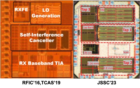
In wireless transceivers, transmitter (TX) and receiver (RX) either share the same frequency band but operate in different time slots (TDD), or share the same time slot but operate in different frequency bands (FDD). A commercial, simultaneous full-duplex (FD) radio sharing identical time slots and frequency bands for the TX/RX pair is still be to realized because of the self-interference (SI) from the TX that is several orders of magnitude stronger than the desired signal at the RX. Realizing such SI cancellation has been hitherto very challenging, because not only does it demand broadband cancellation in amplitude, phase and group delay of the echo signals, but also require such a cancellation circuit to be linear, low-noise and ultra-compact for a mobile form factor.
We recently demonstrated a self-interference cancellation IC with a bandwidth of 80 MHz for a linear, tunable, compact, and fully-integrated FD implementation [ElSayedRFIC16, ElSayedTCAS19]. Another narrowband canceller for long-delay Low-Power Wireless Area Networks (LPWAN) applications achieved up to 70-dB of RF Cancellation.
Our current research is focussed on the applications of full-duplex radios for IoT and other wireless scenarios, including research on both antennas and canceller chips.
Practical Deployment of Silicon Ring Resonator Systems
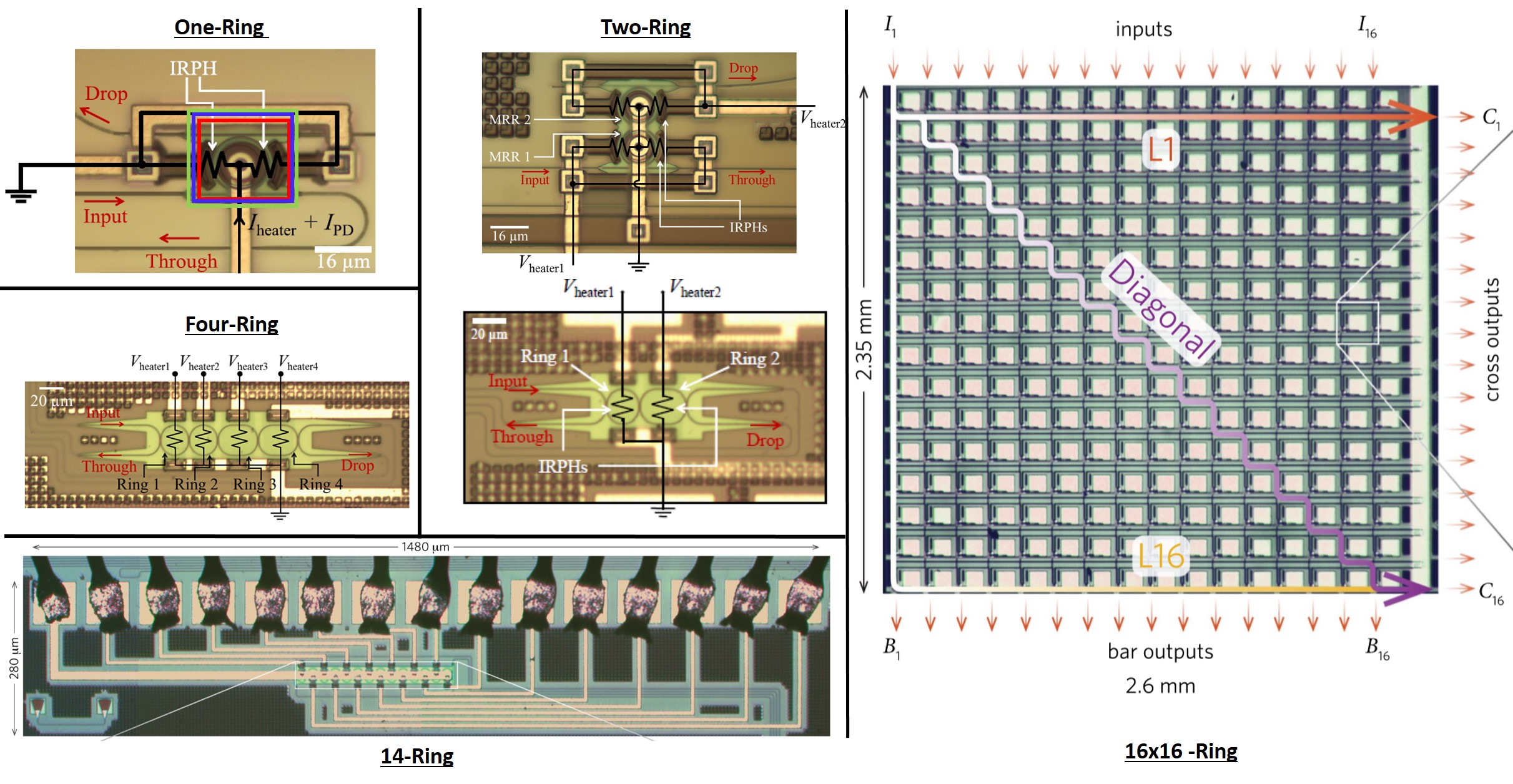
By confining light into resonant structures of um2-scale sizes, microring resonators (MRRs) on silicon photonic platforms allows for low-power, dense, and large-scale manipulation of optical signals on-chip. As a result, MRR-based modulators, switches, and filters bear the promise to be the key building blocks in integrated optical circuits for applications in future data communications, high-performance computing, neuromorphic photonics and sensing. MRR-based modulators promise highly efficient transceivers for datacenters [AhmedJSTQE16, ShomanOFC18]. However, temperature and fabrication variations cause significant shifts in the MRR’s spectral responses, degrading their performance. Conventional solutions to tune MRR require complicated control electronics and several contact pads around MRR, increasing their effective area. These challenges have plagued the widespread adoption of MRR systems beyond the academic world.
We have introduced in-resonator photoconductive heaters (IRPHs) as compact, low-cost implementations to simultaneously sense and tune the resonance conditions of MRRs, without requiring additional material depositions. We have demonstrated automatic tuning and stabilization of one- and two-ring filters [JayatillekaOFC16, JayatillekaOpEx15], four-ring Vernier filters [JayatillekaOFC17, JayatillekaJLT17], and higher-order coupled-optical-resonator-waveguides (CROWs), using simple algorithms. These include record tuning demonstrations for 37.6 nm wavelength range and 65 oC temperature variation. Recently, we demonstrated some of the most complex and largest MRR systems [Jayatilleka-ShomanOptica19].
We have also recently demonstrated a compact microring modulator with tunable extinction ratio to compensate for fabrication uncertainties [ShomanOFC18].
Our ongoing research is focussed on controlling segmented-modulators.
Simultaneous Full-Duplex Electrical Links:
High-speed Input/Output (I/O) data links are used to communicate between microprocessor, memory, hard drive, external plug-and-play devices, etc. Our group is currently investigating low-power links for accelerators and silicon interposer applications, as well as high-performance supporting PAM4 and other advanced modulation schemes. A recent work [YuanTCASI20] focussed on simultaneous full-duplex electrical links, where data is transmitted and received at the same time on the same wireline channel.