~ Abdelrahman H. Ahmed. 9/2015 ~
Virtuoso is a schematic and layout editor software from Cadence.
1 Environment Setup and starting Cadence Virtuoso
The objective of this section is to learn how to get the environment ready for the tool, take care of the licensing issues, and start the tool.
1.1 Virtuoso working Directory
In your Cadence tools directory, created in “RTL Compiler tutorial” section 1, descend into a folder called “cds”. This folder will be the working directory for the Cadence Virtuoso.
1.2 Source the setup file and run Cadence
In the working directory source the provided Setup file. Sourcing this file will take care of all the needed environment variables, and all the licensing as well. After sourcing the setup file, launch the tool.
>> source ../setup_local.csh
>> virtuoso –log Mylog&
>> source /CMC/scripts/kit.gpdk45_OA_v5.csh
>> virtuoso -log myvit.log &
After running the previous lines Cadence should open its main window as in Figure 1, also known as Command Interpreter Window (CIW). Read the log in that window to make sure that everything went well with no errors or warnings.
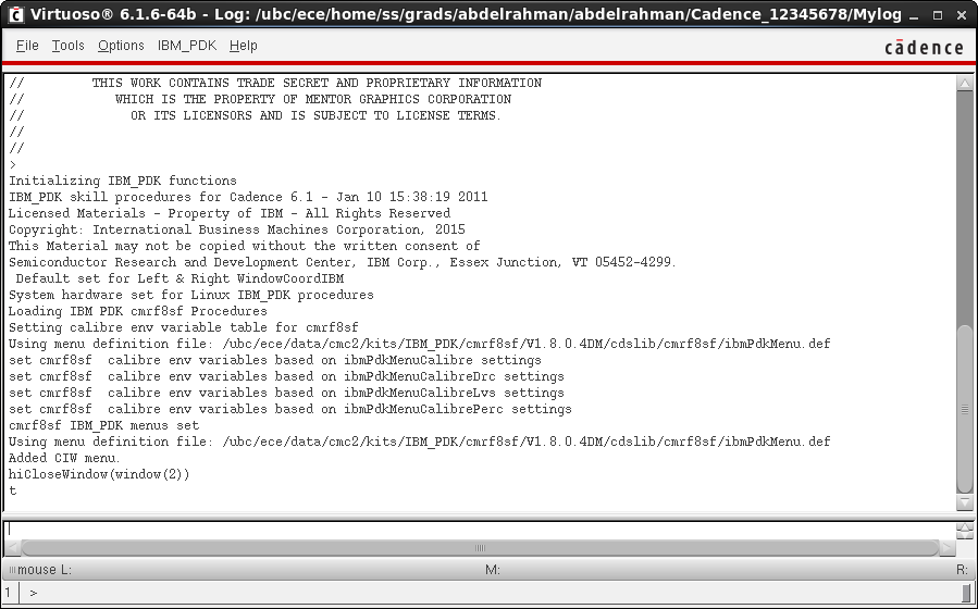
Figure 1 Cadence Virtuoso’s CIW.
2 Starting Virtuoso layout editor
For an error-free schematic, that has only PDK elements and IO pins, open virtuoso schematic editor. In the schematic editor window go to <Launch -> Layout XL>. A “Startup Option” window will open. For ‘Layout’ select Create New and for ‘Configuration’ select Automatic, and press OK. A “New File” window will open. Make sure that the cell name corresponds to your schematic name, and the view is set to be layout, and press OK. Virtuoso Layout editor Figure 2 will open. Start by checking the drop down menus and the GUI buttons to familiarize yourself with the tool.
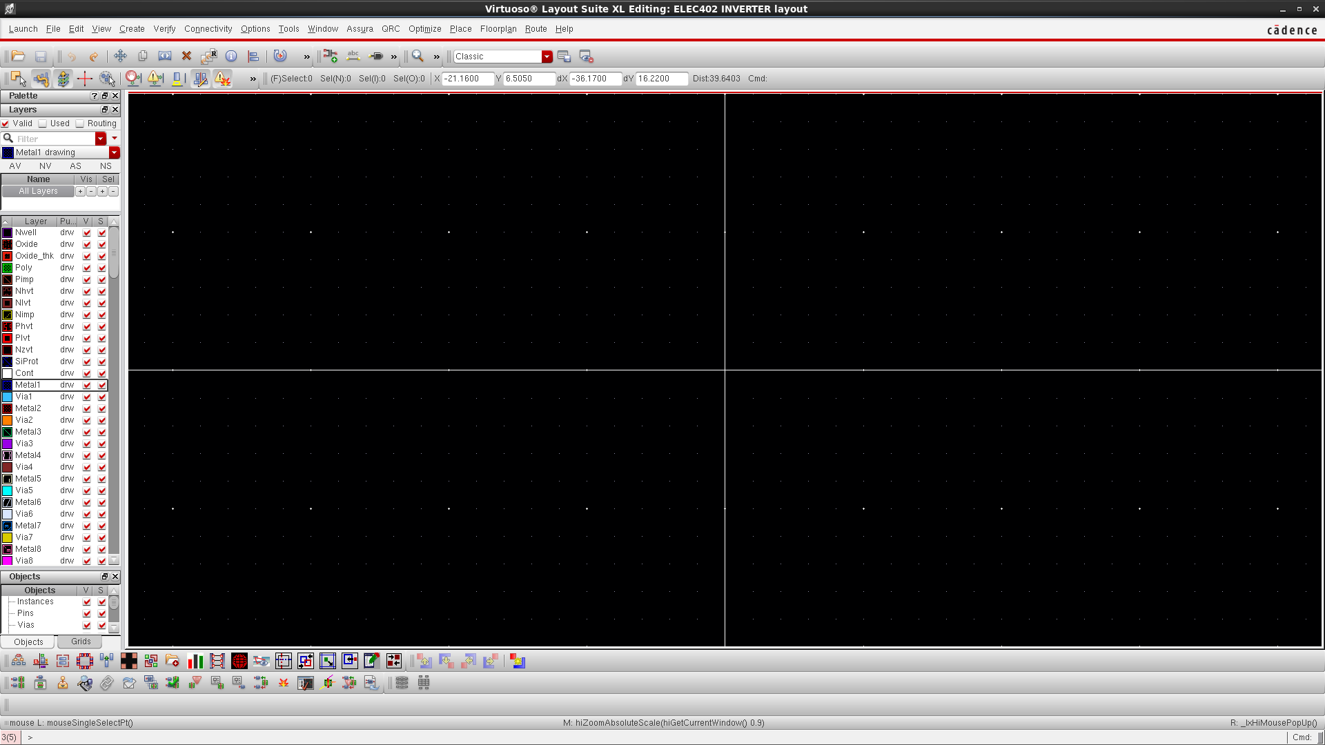
Figure 2 Virtuoso Layout Editor.
To modify the display and the snap options go to <Options -> Display>. Select your preferred options and keep in mind that your minimum snap spacing should match that of the used PDK to avoid Design Rule Check (DRC) errors. [Should be multiple of 0.005 for this GPDK]
3 Cell layout
3.1 Generate used devices from schematic
In this step you will be generating the layout of sub-cells used in building your cell. In the case of an inverter, the generated sub-cells are 1 NMOS, 1 PMOS, and 4 IO pins. You can instantiate these sub-cells like what you did before in the schematic editor. Another way is to ask virtuoso’s assistance in generating the sub-cells. In the layout editor, go to <Connectivity -> Generate -> All From Source>. The “Generate Layout” window will open. Please make sure to select the options as shown in Figure 3, and press OK.
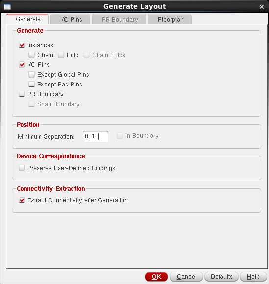
Figure 3 ‘Generate Layout’ window.
Note that the sub-cells have been added to the layout editor window as shown in Figure 4 left. The devices are shown as black boxes, and to view the layers inside each sub-cell press <Shift+F> as shown in Figure 4 right. To go back to boxes view press <Ctrl+F>. Familiarize yourself with the used layers, and use the Palette on your left-hand-side to assist you.
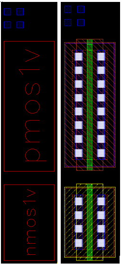
Figure 4 Left (Sub-cells with boxes view). Right (Sub-cells with all layers visible).
3.2 Floorplan and route
Start moving stuff around to match your floorplan. Note that virtuoso assists you by showing virtual connections between nodes as shown in Figure 5. Also, when selecting a sub-cell in the layout editor, note that it will be automatically selected in the schematic editor. To draw a ruler press <K>. To erase all rulers press <Shift+K>.
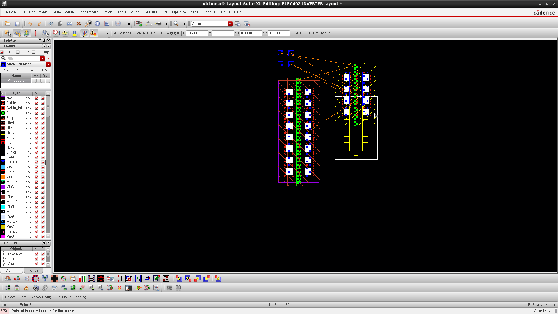
Figure 5 Moving sub-cells.
Finalize the placement and the routing according to your project requirements. Keep in mind that you always want to minimize parasitics generated by connections. Figure 6 shows layout of an inverter.
Notes:
- For a connection to switch between two layers a Via has to be used. To create a Via press <O>. Set the needed options, and make sure that the ‘Via Definition’ field corresponds to the needed transition. For example, to switch between the Poly layer and Metal 1 select [M1_PO].
- For reliability considerations, a minimum of two Via cuts should be used at every transitions.
- To avoid latch up problems, bulk connections should be used. For NMOS use [M1_PIMP Via] and connect it to GND, and for PMOS use [M1_NWELL Via] and connect it to VDD.
- Using “text-drw” layer add labels to all your layout ports as shown in Figure 6.
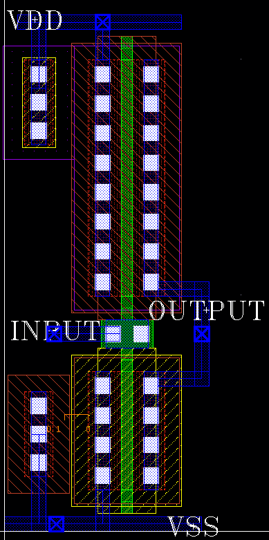
Figure 6 CMOS inverter full layout.
4 Verification and checks
In this section you will be checking that your layout satisfies the fabrication constraints through the Design Rule Check (DRC). Also, you will be checking that both the layout and the schematic match through the Layout Versus Schematic check (LVS). For both checks Cadence’s Physical Verification System (PVS) will be used.
In the layout editor window go to <Launch -> Plugins -> PVS> which will add a new menu for PVS.
4.1 Design Rule Check (DRC)
To start the DRC tool go to <PVS -> Run DRC>. In the DRC window shown in Figure 7 go to <File -> Load Presets> then browse to “virtuoso.drc_preset” and press Submit.
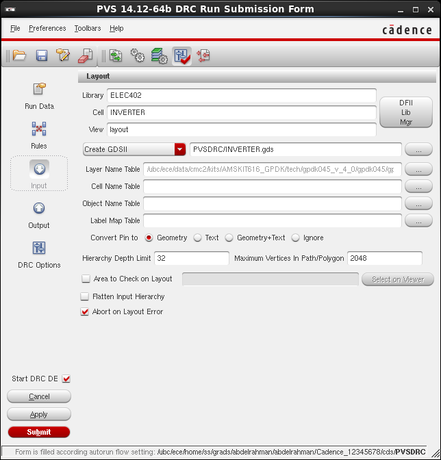
Figure 7 DRC run window.
After running DRC “DRC Debug Environment” window will open Figure 8. In that window you will see all the violations in your layout along with brief explanations. Work on your errors and ReRun from the “PVSDRC” window, Figure 9, until you get a clean design with zero errors.
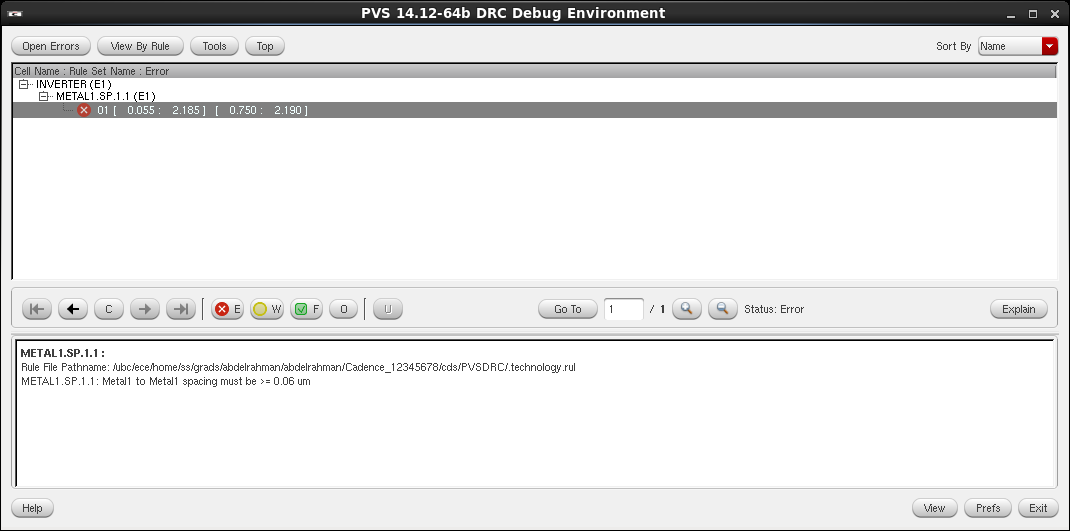
Figure 8 DRC Debug Environment.
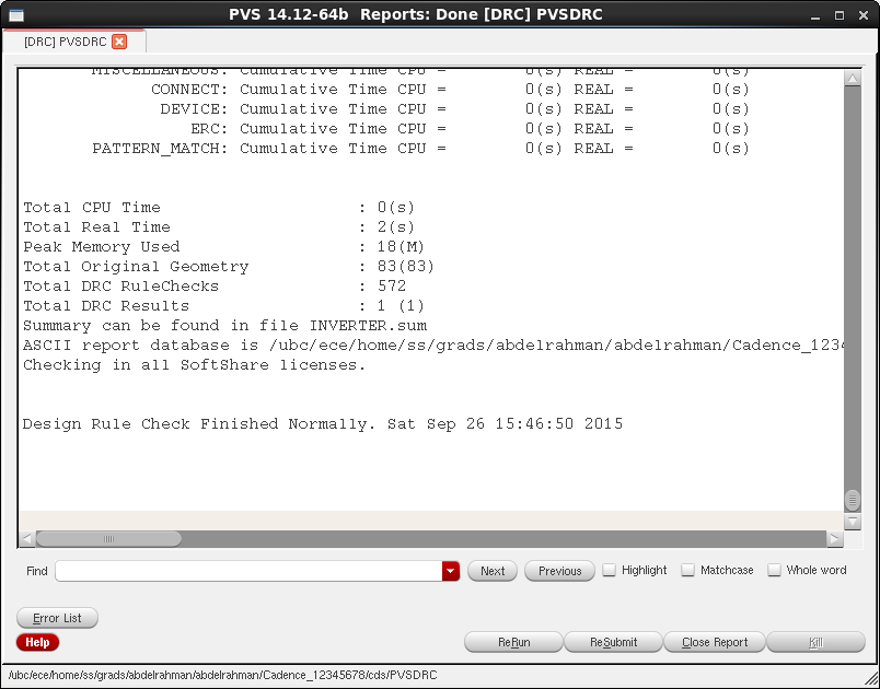
Figure 9 PVSDRC report window.
4.2 Layout Versus Schematic (LVS)
To start the LVS tool go to <PVS -> Run LVS>. In the LVS window shown in Figure 10 go to <File -> Load Presets> then browse to “virtuoso.lvs_preset”. Go to Output tab and make sure that “Create Quantus QRC Input Data” is checked, and press Submit.
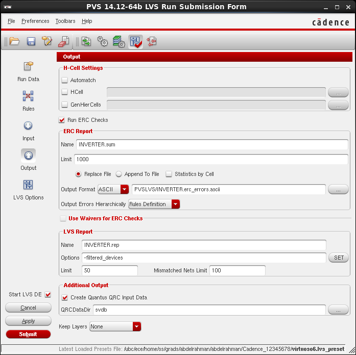
Figure 10 LVS run window.
After running LVS “LVS Run status” window will open Figure 11. Press Yes to open the “LVS Debug Environment” window Figure 12. In that window you will see all the violations along with brief explanations. Work on your errors and ReRun from the “PVSLVS” window, Figure 13, until you get a matched design with zero errors.
![Figure 11 LVS Run status: [Left-Mismatch] and [Right-Match]](https://sudip.sites.olt.ubc.ca/files/2015/09/l11.png)
Figure 11 LVS Run status: [Left-Mismatch] and [Right-Match]
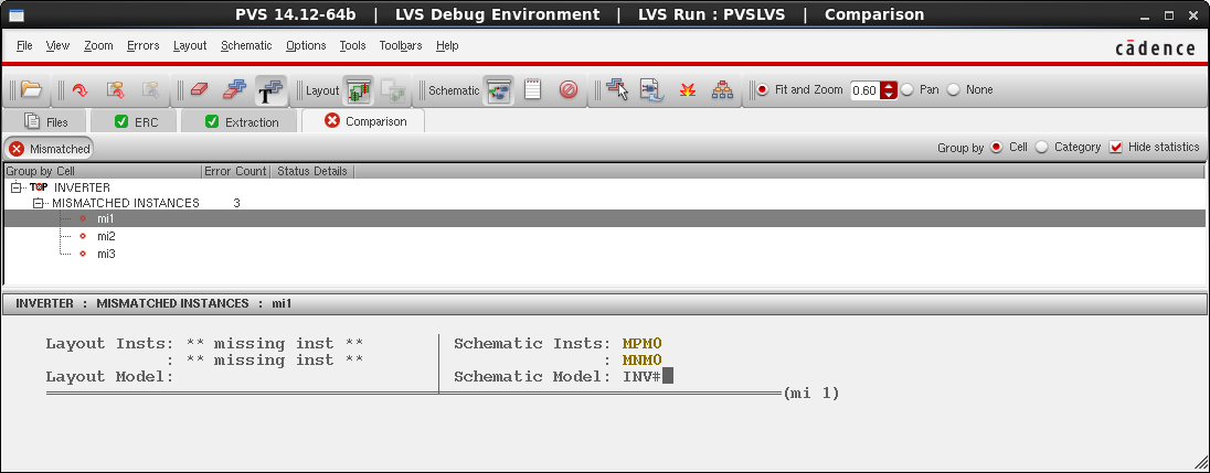
Figure 12 LVS Debug Environment.
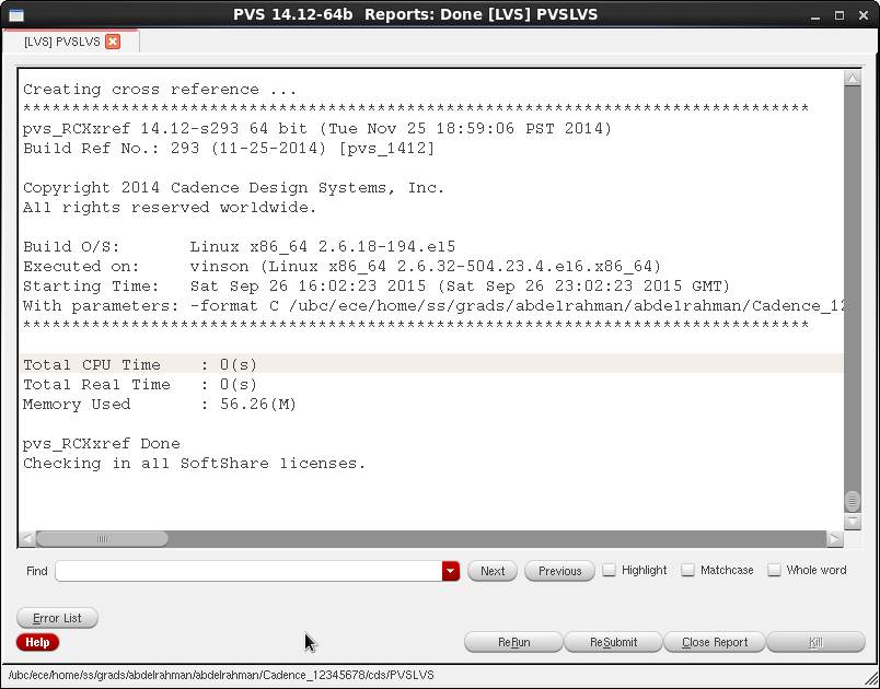
Figure 13 PVSLVS report window.
5 Parasitic Extraction and Post Layout Simulation
5.1 Run QRC extraction
After passing LVS your layout will be ready for extraction. In the layout editor window go to <QRC -> Run PVS-QRC>. In the “QRC (PVS) interface” window, make sure that the cell name and the technology fields are right, and press OK. In the “Parasitic Extraction Run Form” make sure to set the fields as shown in Figure 14 to Figure 16. Press Ok and wait for the tool to do the extraction and give you the completion notification shown in Figure 17.

Figure 14 Parasitic Extraction Run Form (Setup).
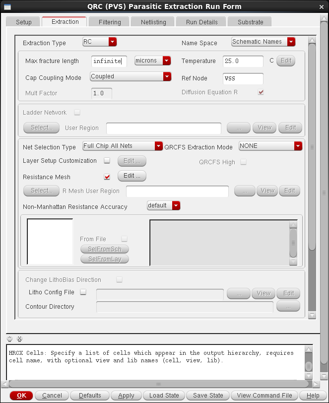
Figure 15 Parasitic Extraction Run Form (Extraction).
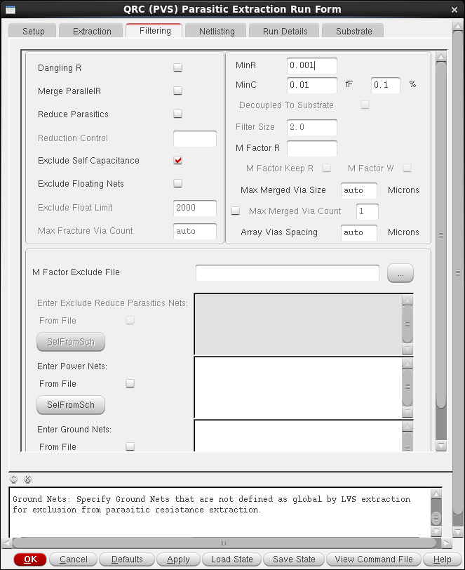
Figure 16 Parasitic Extraction Run Form (Filtering).
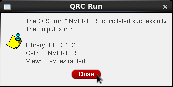
Figure 17 QRC Run Completion Notification.
5.2 Display parasitic associated with nodes
After extracting the layout note that a new cell view named “av_extracted” was added in the Library manager. To show the summation of capacitance associated with each node go to the schematic editor window and go to <Launch -> Plugins -> Parasitics>. In the Parasitics menu go to Setup. In the “Setup Parasitics” window, make sure that all the fields are set similar to Figure 18 and press OK.
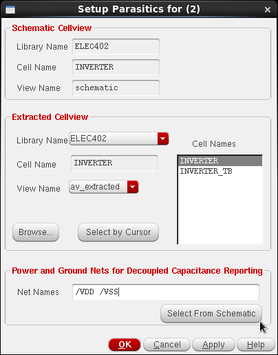
Figure 18 Setup Parasitics.
Go to <Parasitics -> Show Parasitics>. Note that the tool added the summation of capacitance associated with each node to the schematic as shown in Figure 19.
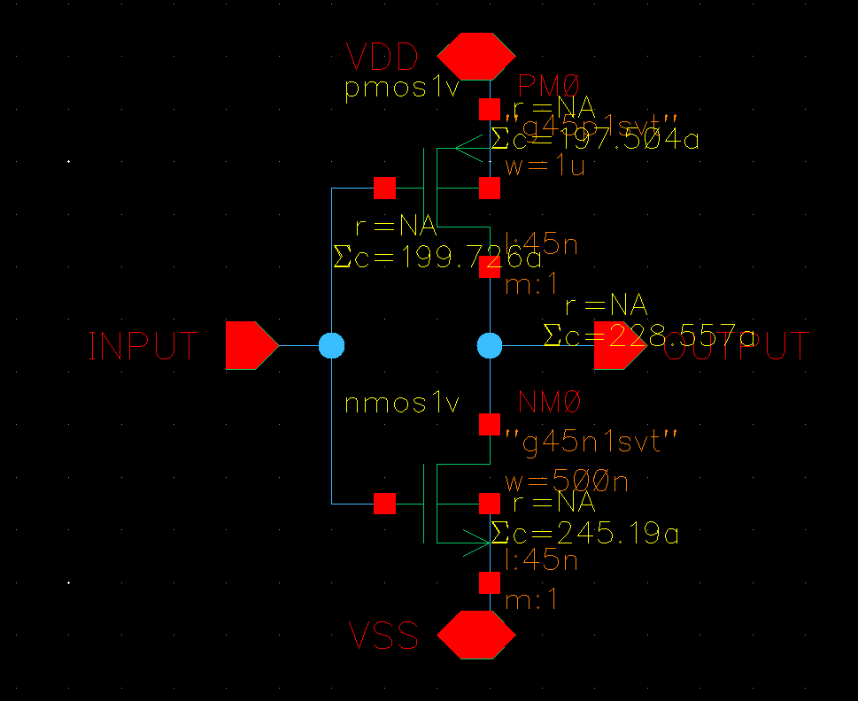
Figure 19 CMOS inverter with the annotated parasitic capacitance.
5.3 Post-layout Simulation
After extracting the layout all the simulation done in “Cadence Virtuoso – Schematic & Simulations – Inverter (45nm)” tutorial should be repeated to include the parasitics’ effect. To do so, you will have to let the simulator know that you want to use the extracted view coupled with the TB netlist, which is done through the “config” view. From the library manager create a new cell view for your TB with the Type field set to “config” as shown in Figure 20. The “New Configuration” window will open. Modify the fields, use the AMS template, and add the “av_extracted” to the View List as shown in Figure 21.

Figure 20 Create config view for the TB.
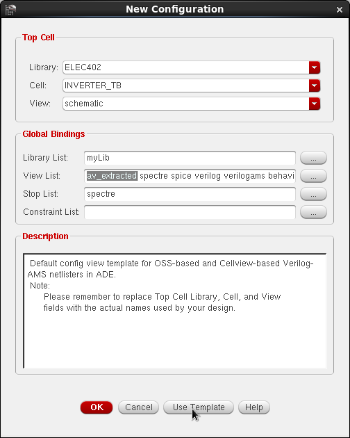
Figure 21 New Configuration.
In Virtuoso Hierarchy Editor, set the View to use for your cell to be “av_extracted” and press “Recompute the hierarchy” as shown in Figure 22. Press Open to open virtuoso schematic editor with in the config view and repeat all the needed simulations. How did the results change?!
Note: Always make sure that the word “Config” exists in the schematic editor window’s name, and the ADE window as well as show in Figure 23.

Figure 22 Virtuoso Hierarchy Editor.
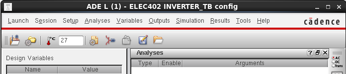
Figure 23 ADE in “config” view.